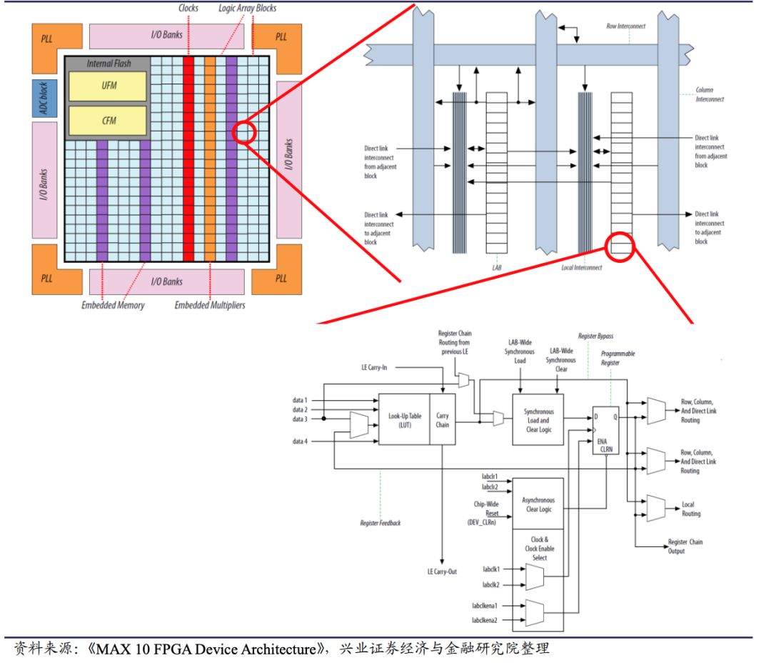
时间:2025-10-20 来源:FPGA_UCY 关于我们 0
答案对人有帮助,有参考价值
如果引脚未连接到FPGA封装内部,请不要将其连接到PCB上的任何内容。如果您的设计未使用该引脚,也不要将其连接到PCB上的任何内容。
这些工具将在所有未使用的IO引脚上实例化内部上拉,您不必担心,我们会为您处理。
此外,对使用的任何输入引脚都没有任何伤害,并且悬空。
Noite确定您过去遇到的“噪音”问题,但FPGA设备设计用于处理所有IO引脚上的中间电压,这在许多应用中通常都存在。
取一些未使用的IO引脚,并将它们连接到接头或引脚字段非常有用,这样当您需要调试时,您可以轻松地将信号路由到这些备用引脚之一。
谢谢和RegardsBalkrishan -----------------------------------------------
---------------------------------------------请将帖子标记为
一个答案“接受为解决方案”,以防它有助于解决您的查询。如果一个帖子引导到解决方案,请给予赞誉。
以上来自于谷歌翻译
以下为原文
If the pin is unconnected internal to the FPGA package, do not connect it to anything on your pcb.
If the pin is unused by your design, also do not connect it to anything on your pcb. The tools will instantiate an internal pullup on all unused IO pins, you do not have to worry about it, we take care of it for you. Also, no harm is done to any input pin that is used, and left floating. Noite sure what "noise" issues you have had in the past, but the FPGA device is designed to handle intermediate voltages on all IO pins asa that is normally present in many applications.
It is very useful to take a number of unused IO pins, and wire them to a header, or a pin field, so that when you need to debug, you may easily route a signal out to one of these spare pins.
Thanks and Regards
Balkrishan
--------------------------------------------------------------------------------------------
Please mark the post as an answer "Accept as solution" in case it helped resolve your query.
Give kudos in case a post in case it guided to the solution.